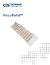
CTS printed piezo thick film is the ideal material choice for miniaturized sensors and transducers. Based on our PZT ceramic formulations, piezoelectric thick film can be deposited onto several industry-common substrates including silicon, alumina and porous ceramics. For flat surfaces, the deposition is carried out by means of standard screen printing. In case of more complex surface structures, a unique printing method, akin to pad printing, is used, enabling deposition of active film layers on substrates with a radius of curvature down to 10mm.
As our expertise grows to encompass additional substrates, we will happily help you develop and produce new technologies for your application. If you have a particular substrate or material in mind, feel free to contact us with details of you specific challenge.
Reach out to us with any questions. We're happy to help.
Contact Us
Results Updated
19 Results Listed
Application Note / Tech Brief
Brochures / Catalogs
Filters
CTS can help decide on material properties to deliver products that meet the unique requirements of your project. Work with a technical expert to begin your design today.
Let's Talk